Notes on the Design and Manufacturing Process of Single-Sided PCBs Using KiCad
This article explains the end-to-end workflow from schematic creation and board design to Gerber output and CNC milling, using practical examples with KiCad and KiCad plugins (Freerouting, pcb2gcodeGUI). Along each step, we also share tips to help streamline your work.
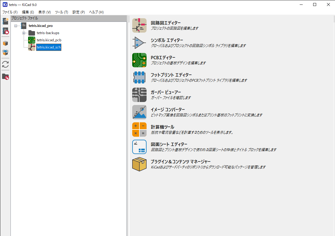
1. Working in the Schematic Editor
-
Component Placement and Wiring
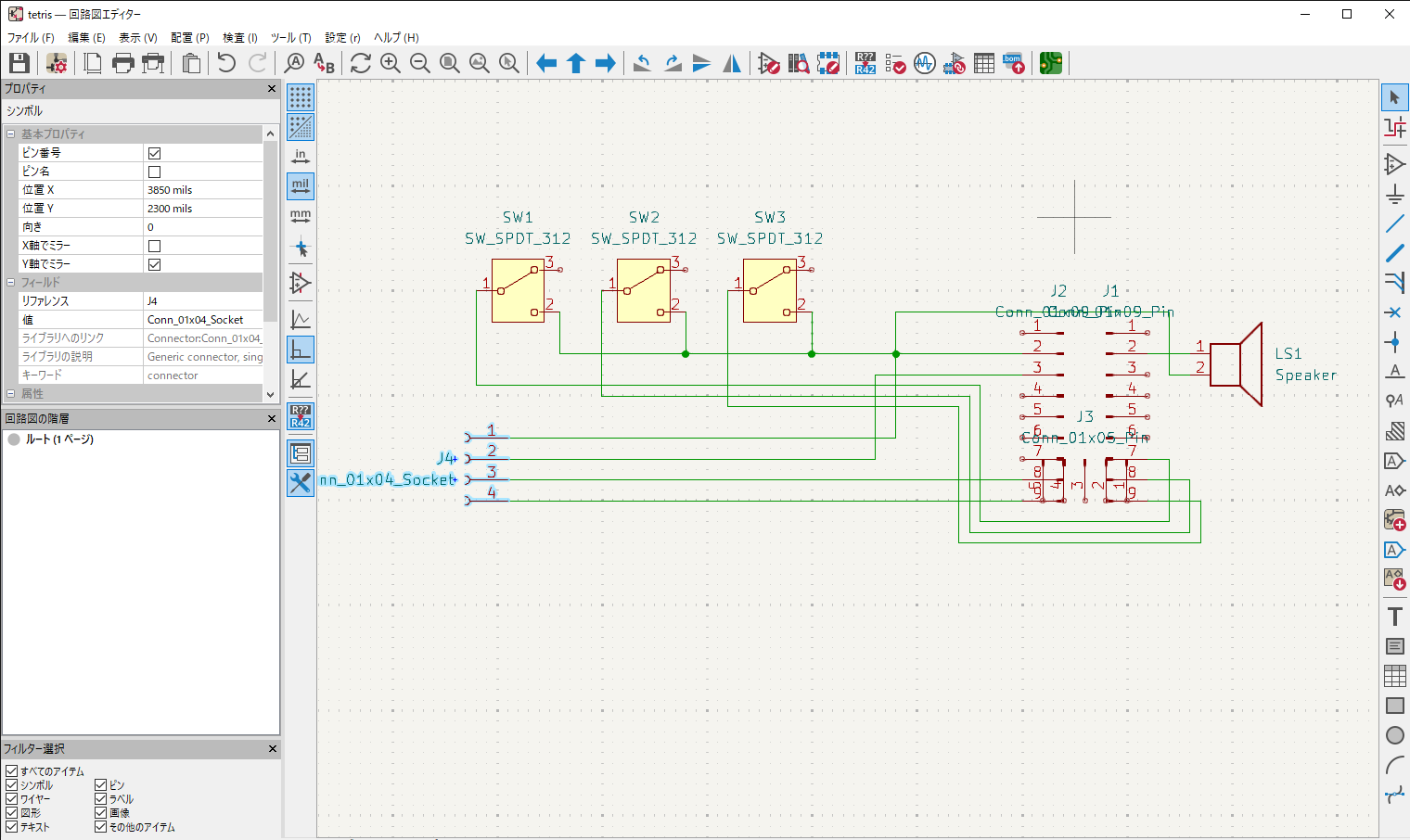
First, launch the KiCad schematic editor, select the necessary components from the libraries, and place them. Wire between the components to create the blueprint for the entire circuit.

-
Assigning Footprints
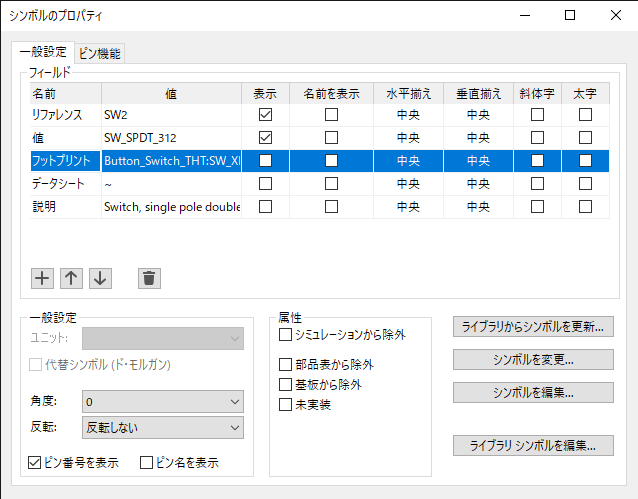
Right-click each symbol (component) and assign the appropriate footprint to the footprint property via the properties dialog. This ensures that the physical components are positioned correctly when later transferred to the PCB editor.

-
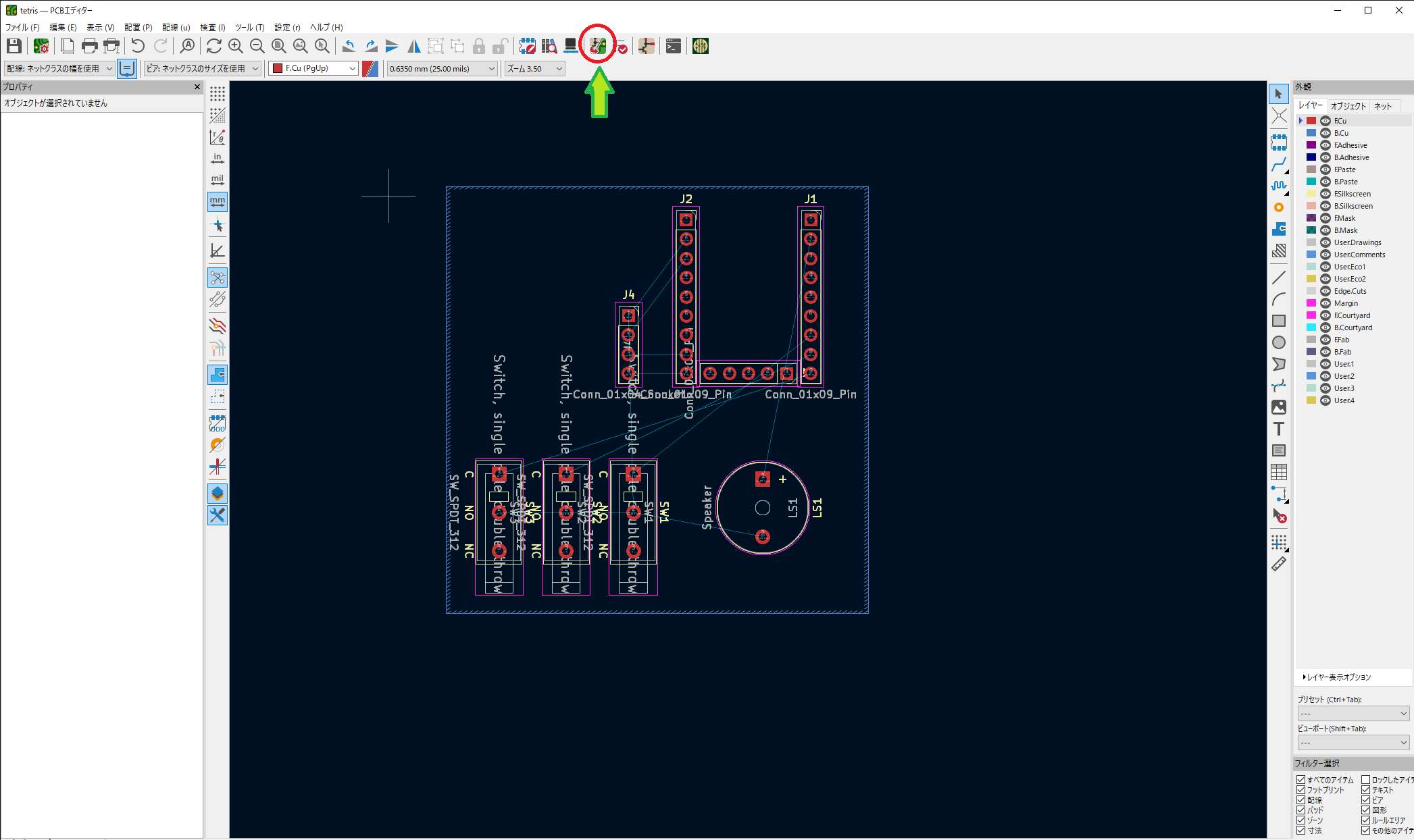
Launching the PCB Editor and Updating the Board
Once the schematic is complete, launch the PCB editor. By clicking the “Update PCB from Schematic" button in the schematic editor, the components and planned trace routes defined in the schematic are transferred to the PCB editor. If configured and wired correctly, the components and their connection patterns will appear on the screen.

2. Layout Work in the PCB Editor
-
Selecting the B.Cu Layer
Before starting work, select the [B.Cu (Back Copper)] layer to prepare for working on the backside of the board. -
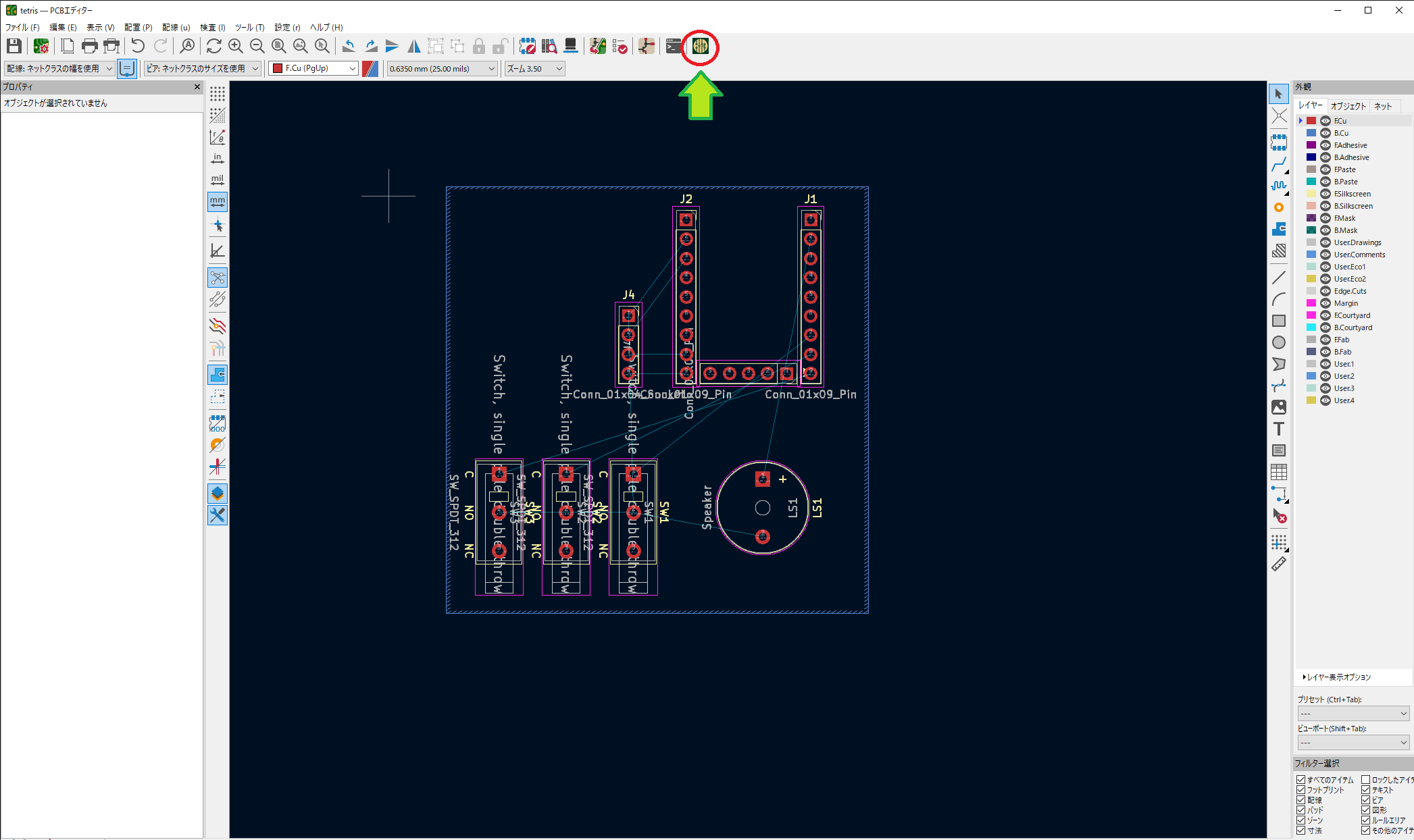
Launching the Freerouting Plugin
Next, launch the Freerouting plugin and perform automatic routing. *Note: You need to install Freerouting from the Plugin and Content Manager on the KiCad home screen.
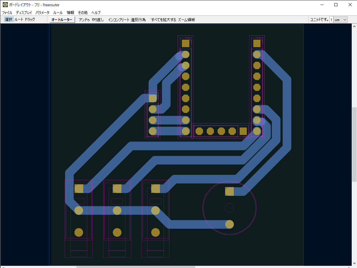
- Clicking the autoroute button here will automatically calculate the routing.

-
Modify the trace width for “kicad_default" under Rules > Net Classes to your preferred size.

- Clicking the autoroute button here will automatically calculate the routing.
-
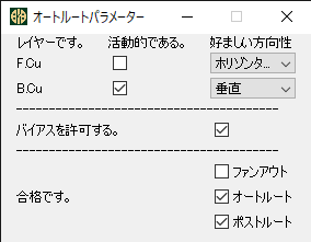
Autorouting Settings for Single-Sided PCBs
For single-sided PCBs, limit the target layers to F.Cu or B.Cu only under Parameters > Autoroute Settings. Unchecking unnecessary layers improves work efficiency.

-
Deleting Unwanted Tracks
If there are incorrect tracks, select [Edit > Delete Globally…], choose “Tracks and Vias", and click OK to delete only the tracks. -
Configuring Filled Zones
After routing is complete, use the [Add Filled Zone] tool to define the fill area for the internal copper planes.
Next, select [Edit > Fill All Zones] to actually fill the designated area. -
Setting Board Edges
To indicate the outline of the board, select the Edge.Cuts layer and accurately draw the edges using the rectangle tool.

3. Exporting Gerber and Drill Files
-
Saving and Plot Settings
First, save your work and select [File > Plot].-
Specify “B.Cu" and “Edge.Cuts" as the layers to include, and set the output format to Gerber.
-
-
Generating Gerber Files
Running the plot will generate the respective .gbr files for the B.Cu and Edge.Cuts layers. -
Creating Drill Files
Next, select [Generate Drill Files].-
Choose the option to merge PTH (Plated Through Hole) and NPTH (Non-Plated Through Hole) into a single file, and generate the .drl file.
-
4. Generating G-code from PCB for the CNC Machine and Milling
-
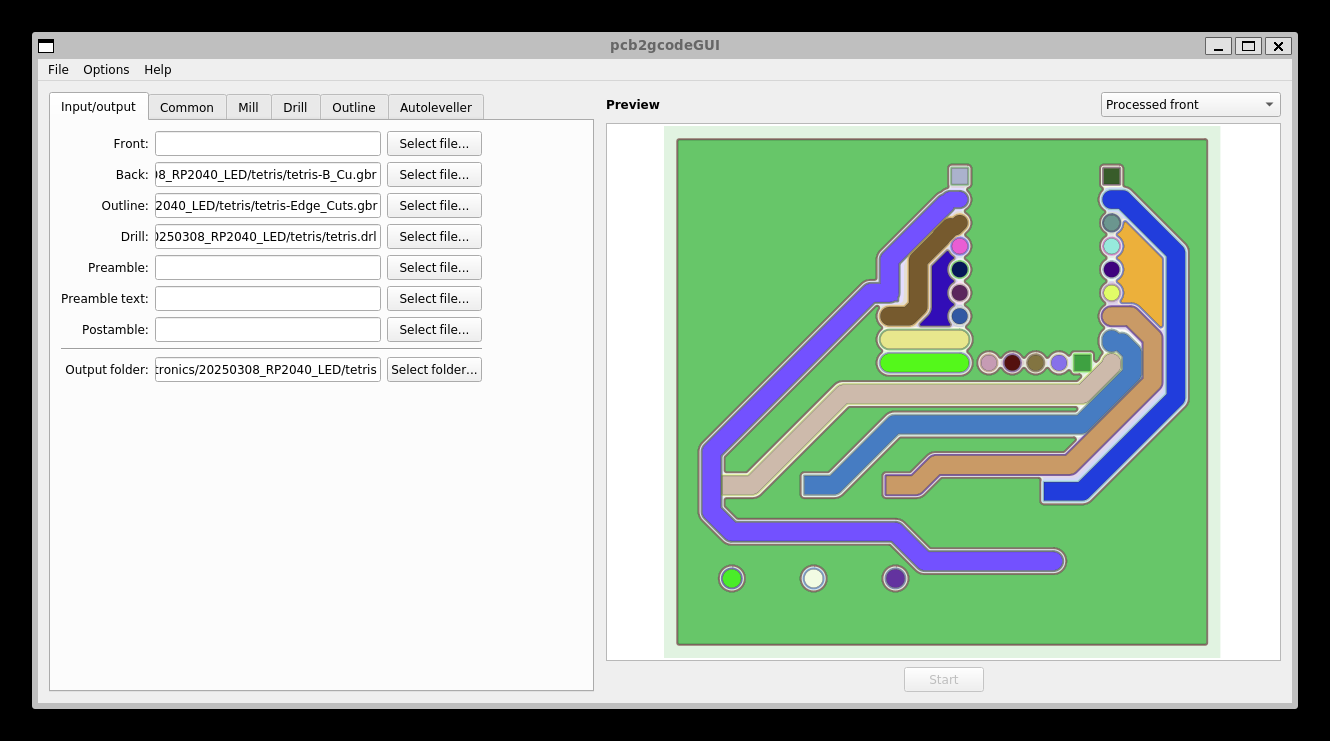
Launching pcb2gcodeGUI
Run pcb2gcodeGUI in the WSL2 environment. *Note: pcb2gcodeGUI must be installed in WSL2.-
Here, set B.Cu to Back, Edge.Cuts to Outline, and the previously generated .drl file to Drill.
-
-
Configuring Parameters in Each Tab
Adjust the necessary settings in each tab within pcb2gcodeGUI, and finally click “Start" to generate the G-code file.

-
Milling with the CNC Machine
Finally, load the generated G-code file into the CNC machine and begin the actual milling process. This physically brings your designed PCB to life.
Conclusion
In this article, we covered the entire procedure using KiCad, ranging from circuit design and PCB layout to outputting Gerber and drill files, and finally generating G-code with pcb2gcodeGUI for CNC milling. We also touched upon detailed settings and plugin usage for each step, so we hope this serves as a helpful reference when tackling similar projects.
In future articles, we plan to dive deeper into more detailed explanations of each setting and troubleshooting tips. Be sure to apply these steps to your own projects for efficient PCB fabrication.